NEW UPDATED POST!
Well. We all know about the “new” Phase5.. he sold me 2 of the Blizzard PPC2 PCBs that I found out was faulty.. no ground connected. and he refused to refund or send new working pcbs.
And at Amiga32 he showed the Blizzard 1260 PCBs. saying that they would go to production any day.
now still one year after.. no production. so this summer I started to actually do a reverse engineer of it, just like I done with the A3640 and Amiga 1200..
Is this ILLEGAL? well.. simply put: no. especially if the the board states that it IS a copy and not claiming to be the real thing. Something I never done in any of my work.
NO original files was used, all is a manual work. Compare making spareparts for your Volvo. fully ok!
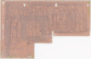
So starting with a B1260 with all components taken off: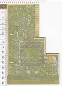
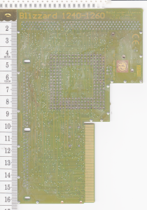
First step is to make the copper more visible:
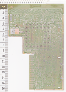
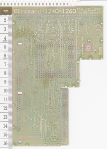
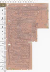
BUT! Thing is. SPRINT that I am using as it is nice to draw traces above a scanned picture. actually only handles 4 layers. ALSO only allow scanned pictures on top and bottom layers. I need to go down to the inner layers first. do them as top/bottom layers and then move them to the internal layer. lets show the INNER layers.. and HOW do I do this? simply sand more… 🙂 and as this PCB is quite “see through” I just sand off the copperlayer you see.
Now I just need to scan this. and do all tracing.
Anyway now I have finally done boards of this. and got it to boot. With memory. AND also with SCSI module and memory. so it is tested with full 256MB of ram and SCSI Controller (not booting from it due to lack of cable 🙂 )
files? suure as usual!:
https://www.hertell.nu/webfiles/Blizzard1260.zip
TLDR; FILES IS ABOVE!
Locator found at: http://locator.reamiga.info/locator.php?project=Blizzard1260
There are 2 sprintfiles! the “Blizzard1260Layers.lay6” is the file for all traces, outline, drill holes etc.
The file “Blizzard1260Inner.lay6” is ONLY for GND+Power planes. the rest should be ignored.
Remember if yo do ANY changes you need to move ALL vias etc to EXACT positions in both files or you WILL have shorts.
If you want to use those files for troubleshooting. use the demoversion of Sprint layout.. use the testfunction (hotkey X) and click on a trace/via and it will be highlighted.
names of signals is based on pinout of connectors etc.
THERE ARE NO WARRANTY OF ANYTHING HERE! you do it on your own! I leave NO support NO NOTHING!
BUTBUT! CPLDS?????
Sorry. they are not reversed. you still will need to have a donorcard. like a board someone screwed up 040-060 upgrade or so..
ENJOY!
Hi John,
first of all, thank you for all this painstaking work! It’s really appreciable to see people like you keeping this old hardware alive.
Now, I have a very specific problem, and I’m a bit lost here:
I recently acquired a Blizzard 1260 (converted from 1240) along with a 32MB SIMM and a Rev.5 CPU. The conversion was very badly done. Huge solderblobs, charred soldermask, flux residue everywhere. However, I’ve eben able to clean up most of the mess and have the card running rock stable at 66 MHz.
A few days ago, I bought a SCSI Kit IV on Amibay. Seller states it’s fully teated and I believe him. The SCSI part is properly detected and shows latest ROM version 8.5. BUT, whatever size of SIMM module I put in the SCSI Kit, only 2 MB of it are being detected.
Can this be due to a broken trace on the 1260? Do you perhaps have any hint as to where to look?
Thank you very much in advance!
Best,
Torsten
havent investigated in that yet. so no idea yet. I will do a complete schematic of the blizzard 1260 someday
Hi, great job.
I’m just comparing reversed engineered schematics with my faulty 1260 card. I’d like to provide corrections.
I also have faulty Bppc card.
I’d like to try some repairs. I’m looking for any help.
I’m thinking about moving chips from my faulty BPpc card to your pcb without ground and building ground layer from reverse engineered my faulty bppc pcb.
if you have corrections. please tell me before I do a PCB run 🙂
bppc. have slight plans of that aswell.. someday maybe
Do far I have found 2 errors.
I have gerbview tool only, so I’m using paper printouts :-).
How do you want me to provide corrections?
Yes please.. Send it via mail (I send you a mail about this)
Have you checked your ground plane?
Hi Chucky and TerrorableFire,
I’m impressed with both of your wor to date.
Not sure if it interests you but I have the following that I’d be prepared to lend out (so long as they aren’t sanded down and I get them back) if you want to reverse engineer I have no issue at all.
Sadly the Gemini is 1 of 2 and I own the lesser of the two prototypes (the one missing some PALs and Amiga custom chips). Dave Haynie did have some of the PAL on his Haynie archive site a while back and I’m sure he’d discuss with you should you contact him about it.
1x Commodore Gemini (the one with less chips of the two prototypes).
1x Cyberstorm PPC – 68060/604e (I believe).
1x Blizzard PPC – 68040 with 603e (I believe),
1x Blizzard 1230
Let me know if you wish to borrow any of these. I’m not on any Amiga forums so I’m only really available via email and I work very odd shifts. I also don’t always see email so if I don’t answer nag me continually until I respond is possibly best approach.
Regards,
Michael
well that would be pointless as the cplds are too hard to crack.. the blizzard was done just “because”
Hi Chucky,
The missing PALs are on the Haynie Archive!
I also have a copy them from Mr Haynie when I bought this from him.
I looked through the documentation Dave sent me (as well as the photos of their location on the board). I would be willing to lend you this to reverse engineer if you are willing/wanting to reverse engineer it; I am a little too scared to mess with something there are only two of. My only catch is I would like it back when you are finished with it.
Let me know what you think?
Michael
Never realised the spelling mistake on PCB mask – “Lisence”.